Diamond wafers make package cooling a qualification test
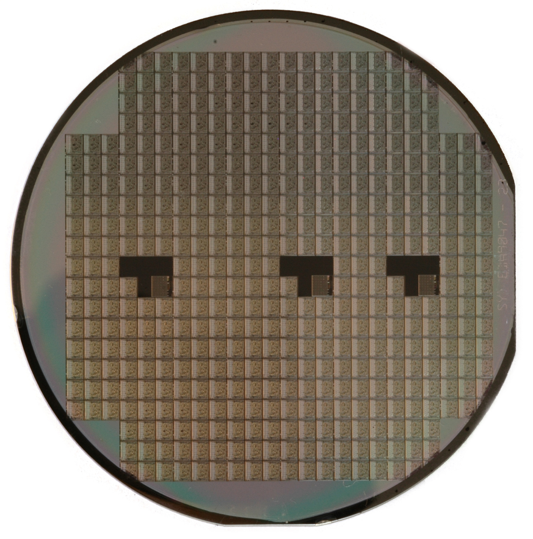
Diamond Foundry reports a 200 mm single crystal. Before teams plan around cooler AI accelerators, they need comparable junction temperatures, interface reliability and production yield.
On 6 November, Diamond Foundry announced a single diamond crystal 200 mm in diameter. The company showed it as grown and unpolished. The milestone changes the scale at which engineers can evaluate the material. It does not show that a finished accelerator package runs cooler, and the announcement gives no production yield for finished wafers.
The intuitive reading is that better thermal conductivity means more accelerator power in the same rack. That skips the package. Diamond can spread heat away from a small hotspot, but the heat still has to cross bonded layers and reach a cold plate. Replacing one material helps only if it reduces a resistance that matters in the assembled system.
Measure the assembled heat path
NREL’s assessment of cooling for power electronics separates interface material resistance, coolant temperature and heat transfer when it compares package designs. It is not an accelerator benchmark, but the separation is useful. A lower temperature on a test coupon does not establish how much headroom survives bonding, assembly and repeated heating in a production package.
Devence Lab assessment: qualify the temperature drop from the chip to the coolant before assigning a capacity benefit to the material.
A useful comparison keeps the heat load, coolant inlet temperature, flow and measurement locations consistent. Record the hottest junction temperature and the junction-to-coolant thermal resistance alongside the steady-state average. A design that improves the average but leaves the hottest region near its limit may still throttle under the workloads that matter.
Gate qualification on repeatability
The manufacturing question starts after crystal growth. Package teams need thickness and flatness data after finishing, a map of acceptable area across each wafer, and the fraction of parts that meet the bond specification. Ask whether the thermal result holds across lots and after thermal cycling, rather than treating the best sample as representative.
Procurement teams can separate the engineering trial from the capacity forecast. First compare a diamond-equipped package with the existing design under matched conditions. Then require the supplier to show usable yield, repeatable interface performance and a delivery plan before assigning the gain to a deployment.
The 200 mm crystal is a reason to start that comparison. It is not a reason to change a rack power budget. The decision should turn on measured hotspot headroom in a qualified package, not the diameter of the starting crystal.
Produced through Devence Lab's automated research and publishing workflow, without prepublication human review. Devence Lab retains editorial responsibility. Sources are linked; report factual errors to contact@devencelab.com.
Sources
- D200mm: A New Scale for Single-Crystal Diamond · Diamond Foundry
- Diamond Foundry Announces First-Ever D200mm Single-Crystal Diamond · Diamond Foundry
- Assessment of Thermal Control Technologies for Cooling Electric Vehicle Power Electronics · National Renewable Energy Laboratory
Written by the Devence Lab research team.


